


For decades, the roles in our industry were clear: semiconductor firms designed chips, and enterprises consumed them. That era is definitely over. A new class of enterprise is emerging—one that is moving from off-the-shelf consumption to custom creation, forging its own silicon to dictate its own destiny.
A perfect storm of forces is driving this shift: the insatiable demands of artificial intelligence, the relentless pursuit of economic efficiency, and the strategic need for supply chain control. And this is forcing leaders to ask: Is our future built on someone else’s hardware, or on our own?
The Catalyst: AI, Economics, and the End of "Good Enough"
The rapid advancements of generative AI have exposed the limits of a one-size-fits-all hardware strategy. The computational power needed for training and running large language models is staggering, with some estimates suggesting it doubles every few months. While general-purpose GPUs are powerful, deploying them for specific workloads at scale creates significant bottlenecks in power consumption, performance, and simple availability.
This has created a compelling business case for custom silicon. Purpose-built Application-Specific Integrated Circuits (ASICs) deliver a significant leap in performance-per-watt for targeted AI tasks. Beyond performance, the economic argument is undeniable. For hyperscalers and large enterprises, custom chips are a powerful tool for data center modernization, driving down the total cost of ownership (TCO) by optimizing for their exact software stack. Ultimately, in an era of growing geopolitical uncertainty, designing one's own silicon is a strategic move to mitigate supply chain risks and assert technological sovereignty.
The Vanguard: How Hyperscalers Forged the Path
The industry’s most dominant players have already demonstrated the profound value of vertical integration at the silicon level. Their investments serve as a playbook for the rest of the industry, proving that owning the chip means owning the performance and economic equation.
- Amazon has leveraged its Arm-based Graviton processors to optimize performance and cost for its AWS customers, while its Trainium and Inferentia chips target the AI/ML workload lifecycle directly.
- Google’s long-standing investment in Tensor Processing Units (TPUs) has given it a formidable, in-house advantage for its AI-centric services, from search to cloud offerings.
- Meta is aggressively pursuing its own path with the Meta Training and Inference Accelerator (MTIA), a clear signal that even social media and metaverse workloads demand custom hardware for future growth.
The Ripple Effect: Custom Silicon Spreads Across Industries
To dismiss this as a "hyperscaler-only" game would be a critical miscalculation. What began in the cloud is now cascading across every major vertical, as leaders recognize that the next wave of innovation must be built on a custom hardware foundation.
We are seeing this ambition take root everywhere:
- Telecommunications: Firms are designing custom silicon to power 6G services and deliver the low-latency processing required for AI-driven edge applications.
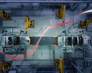
- Automotive: The race to dominate the software-defined vehicle (SDV) is becoming a race to own the underlying chips for autonomous driving (ADAS) and in-vehicle experiences.
- Financial Services: Companies are developing purpose-built chips to gain microsecond advantages in high-frequency trading and to run sophisticated, real-time fraud detection algorithms.
- Healthcare: Specialized ASICs are being created to dramatically accelerate drug discovery, genomic sequencing, and the analysis of complex medical imaging.
The Partnership Imperative: From Chip Ambition to Market Reality
As this ambition grows, leaders are confronting a stark reality: designing custom silicon is monumentally complex. The cost to design a chip at an advanced 5nm node can exceed $500 million, and that figure climbs with each new process generation1. The process demands a rare combination of capital, world-class talent, and deep domain expertise.
This complexity, however, is not a barrier—it is an invitation for a new model of collaboration. For an automotive company, a bank, or a telco focused on its core business, the most efficient and effective path to custom silicon is through a strategic engineering partnership. An expert partner with deep VLSI and system design capabilities can translate specific business needs into silicon reality, providing three critical advantages:
- Accelerated Time-to-Market: Navigating the design and fabrication ecosystem to deliver a functional chip on schedule.
- Access to Scarce Talent: Tapping into a global pool of elite engineering talent without the overhead of building an entire division from scratch.
- Mitigation of Execution Risk: Leveraging proven methodologies to avoid costly design flaws and manufacturing delays.
The Way Forward: The Future is Forged in Silicon
The line between technology consumer and creator has irrevocably blurred. In the era of AI and intense global competition, owning your silicon stack is becoming synonymous with owning your competitive advantage. This shift is also creating massive opportunities for the broader semiconductor ecosystem, demanding new, flexible engagement models from foundries and OSATs prepared for a world of heterogeneous integration.
The question for every leader is no longer if they should consider this path, but who their trusted partner will be on the journey. The future will be led by those who are bold enough to build it, starting from the silicon up.
Endnotes
- Tatiraju, U., Zmora, N., & Lott, C. (2024, June 11). Generative AI for semiconductor design.AWS for Industries.